 KOR
KOR ENG
ENGT. 042.633.9511
Copyright ELTECH Corp.
All Rights reverved.
PCB design, manufacturing and consulting
ELTECH uses its unique technology to provide the best PCB design/consulting.
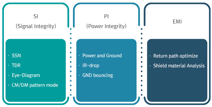
Since PCBs are sensitive to noise, to repair circuits that malfunction due to a high-frequency line design operating at dozens of GHz and to validate the sign attributes on the PCB, it is necessary to perform an analysis using an electromagnetic field analysis tool.
ELTECH uses its unique technology to provide the best PCB design/consulting and to manufacture PCBs optimized and customized to your requirements.


PCB manufacturing specifications
| Description | Standard | Advance | Description | |
|---|---|---|---|---|
| a | Min. Trace Width | Copper Thickness + 50μm (Copper Thickness + 2mil) |
Copper Thickness | 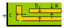 |
| b | Min. Trace to Trace Clearance | Copper Thickness + 75μm (Copper Thickness + 3mil) |
Copper Thickness + 50μm (Copper Thickness + 2mil) |
|
| c | Min. Pad to Substrate Edge (Press Punching) |
Board Thickness + 200μm (Board Thickness + 8mil) | ||
|
Min. Pad to Substrate Edge (Routing) |
150μm (6mil) | |||
| Description | Standard | Advance | Description | |
|---|---|---|---|---|
| a | Min. Diameter of Drilling Hole | 0.20ø (8mil) | 150μm (6mil) | 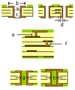 |
| b | Min Diameter of Annular Ring | a +0.20ø/a + 8mil | a +0.15ø/a + 6mil | |
| c | Diameter of Finished Hole |
0.15ø (6mil) | 0.10ø (4mil) | |
|
Internal Ground / Signal Clearance |
150μm (6mil) |
100μm (4mil) | ||
| e | Min. Diameter of Blind Via(Finished) | 0.10ø (4mil) | 0.05ø (2mil) | |
| f | Min. Diameter of Blind Via(Finished) | 0.10ø (4mil) | 0.05ø (2mil) | |
| g | Max. Hole Diameter & Board Thickness for Filled Via with PSR | Diameter | Thickness | |
| h | Max. Hole Diameter & Board Thickness for Filled & Plated Via in Pad | 0.6ø (24mil) | 2.0mm (80mil) | |
| Throwing Power | Diameter | Thickness | ||
| Aspect Ratio | 0.5ø (20mil) | 2.0mmø (80mil) |
| Description | Standard | Advance | Description | |
|---|---|---|---|---|
| a | Clearance of Solder Mask to SMD Pad |
80μm (3.15mil) | 50μm (2.00mil) | 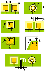 |
| b | Min, Solder Mask Web | 100μm (4.00mil) | 80μm (3.15mil) | |
| c | Clearance between Solder Mask Opening and Annular Ring |
80μm (3.15mil) | 50μm (2.00mil) | |
|
Thickness of Solder Mask |
Max 10μm (Max 0.8mil) | Max 20μm (Max 1.2mil) | ||
| e | Solder Mask Thickness on the Circuit Knee | 4μm (0.1mil) | 8μm (0.2mil) | |
| f | Legend Width | 150μm (5mil) | 125μm (4mil) |
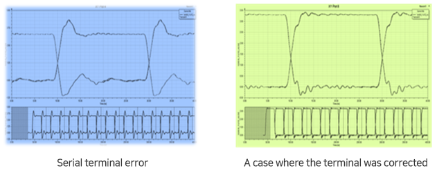
Cases of consulting
It was a case of consulting where the incorrectly designed location of the line’s TX/RX terminal resistance was discovered and corrected.
A case where a serial terminal error was discovered and the terminal was corrected
It was a case of consulting where a TDR analysis was performed to control the s-parameter and impedance demonstrating the line’s delivery, reflection and crosstalk attributes.
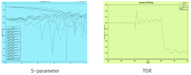
Communication lines such as ethernet and space-wire are important SI analysis targets.
It was a case of consulting where this company performed an analysis.
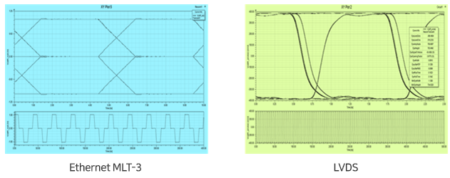
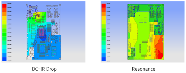
It was a case of consulting where a PI analysis was performed to analyze the PDN and resonance associated with power supply.